- 您现在的位置:买卖IC网 > Sheet目录1994 > DS3106LN+ (Maxim Integrated Products)IC TIMING LINE CARD 64-LQFP
DS3106
12
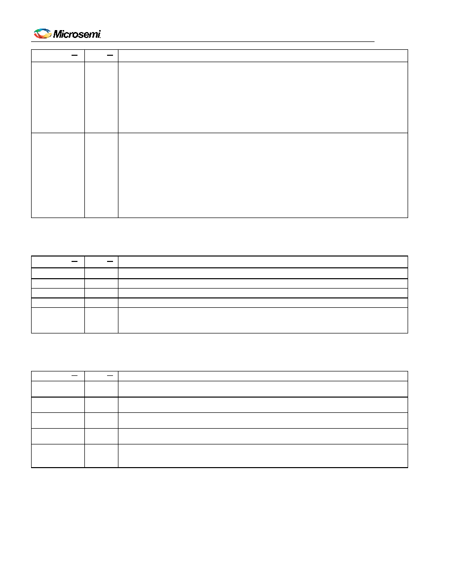
PIN NAME
TYPE
PIN DESCRIPTION
SONSDH/
GPIO4
IOPD
SONET/SDH Frequency Select Input/General-Purpose I/O 4. When
RST goes high the state
After
RST goes high, this pin can be used as a general-purpose I/O pin. GPCR:GPIO4D
configures this pin as an input or an output. GPCR:GPIO4O specifies the output value.
GPSR:GPIO4 indicates the state of the pin.
Reset latched values:
0 = SDH rates (N x 2.048MHz)
1 = SONET rates (N x 1.544MHz)
INTREQ/LOS
O3
Interrupt Request/Loss of Signal. Programmable (default: INTREQ). The INTCR:LOS bit
determines whether the pin indicates interrupt requests or loss of signal (i.e., loss of selected
reference).
INTCR:LOS = 0: INTREQ mode
The behavior of this pin is configured in the INTCR register. Polarity can be active high or
active low. Drive action can be push-pull or open drain. The pin can also be configured as
a general-purpose output if the interrupt request function is not needed.
INTCR:LOS = 1: LOS mode
This pin indicates the real-time state of the selected reference activity monitor (see Section
Table 6-4. SPI Bus Mode Pin Descriptions
PIN NAME
TYPE
PIN DESCRIPTION
CS
IPU
Chip Select. This pin must be asserted (low) to read or write internal registers.
SCLK
I
Serial Clock. SCLK is always driven by the SPI bus master.
SDI
I
Serial Data Input. The SPI bus master transmits data to the device on this pin.
SDO
O
Serial Data Output. The device transmits data to the SPI bus master on this pin.
CPHA
I
Clock Phase. See Figure 7-4.
0 = Data is latched on the leading edge of the SCLK pulse.
1 = Data is latched on the trailing edge of the SCLK pulse.
Table 6-5. JTAG Interface Pin Descriptions
PIN NAME
TYPE
PIN DESCRIPTION
JTRST
IPU
JTAG Test Reset (Active Low). Asynchronously resets the test access port (TAP) controller. If
not used,
JTRST can be held low or high.
JTCLK
I
JTAG Clock. Shifts data into JTDI on the rising edge and out of JTDO on the falling edge. If
not used, JTCLK can be held low or high.
JTDI
IPU
JTAG Test Data Input. Test instructions and data are clocked in on this pin on the rising edge
of JTCLK. If not used, JTDI can be held low or high.
JTDO
O3
JTAG Test Data Output. Test instructions and data are clocked out on this pin on the falling
edge of JTCLK. If not used, leave unconnected.
JTMS
IPU
JTAG Test Mode Select. Sampled on the rising edge of JTCLK and is used to place the port
into the various defined IEEE 1149.1 states. If not used connect to VDDIO or leave
unconnected.
发布紧急采购,3分钟左右您将得到回复。
相关PDF资料
DS3231MZ+
IC RTC I2C 8SOIC
DS3231SN#T&R
IC RTC W/TCXO 16-SOIC
DS3232MZ+
IC RTC W/SRAM I2C 8SOIC
DS3232SN#T&R
IC RTC W/TCXO 20-SOIC
DS3234S#
IC RTC W/TCXO 20-SOIC
DS32C35-33#T&R
IC RTC ACCURATE I2C 3.3V 20-SOIC
DS3911T+
IC DAC 10BIT I2C QUAD 14TDFN
DS4000KI/WBGA
IC OSC TCXO 19.44MHZ 24-BGA
相关代理商/技术参数
DS3107FP000
制造商:Thomas & Betts 功能描述:30A,CON,2P3W,MG,107,125V
DS3107FRAB0
制造商:Thomas & Betts 功能描述:30A,REC,2P3W,MG,107,AB0,125,SC
DS3107MP000
制造商:Thomas & Betts 功能描述:30A,PLG,2P3W,MG,107,125V
DS3107MP00K
制造商:Thomas & Betts 功能描述:30A,PLG,2P3W,MG,107,125V,CC
DS3107MR000
制造商:Thomas & Betts 功能描述:30A,NLT,2P3W,MG,107,125V
DS3107MRAB0
制造商:Thomas & Betts 功能描述:30A,NLT,2P3W,MG,107,AB0,125V
DS3108A14S5S621
制造商:Amphenol Corporation 功能描述:
DS3108A14S6S
制造商:Amphenol Corporation 功能描述: